Fundraising
Supporting deep-tech start-ups in their process of raising venture capital. We maintain a global network of (deep-tech focused) (C)VCs with direct access on partner-level.

The TD Shepherd team has been helping technology companies successfully navigate the maze of corporate finance since 2014. We have successfully completed over 100+ transactions, ranging from fundraising to exit to fund-for-fund and other strategic services within the deep-tech eco-system. Our customers range from early-stage startups, incubators, VCs and CVCs all the way to smaller and larger corporates in the North American and European geography. All these customers share a common feature: being active in the deep-tech eco-system.
TD Shepherd is a deep-tech corporate finance firm that facilitates optimized transactions for its clients. We do this through a unique combination of engineering and commercial expertise and experience. Our Associates are global (including the Silicon Valley, Canada, The Netherlands, Germany and the UK) so we can expand the international reach of our clients to maximize their opportunities.
Our primary focus areas encompass deep technologies, with a particular emphasis on:
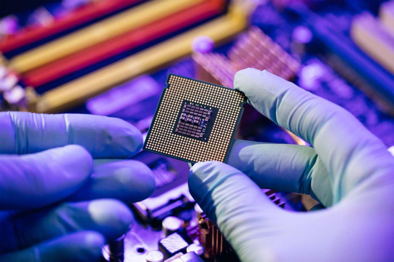
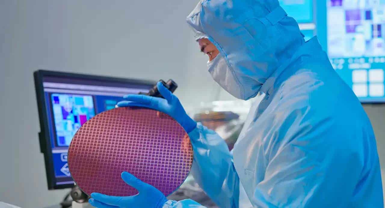
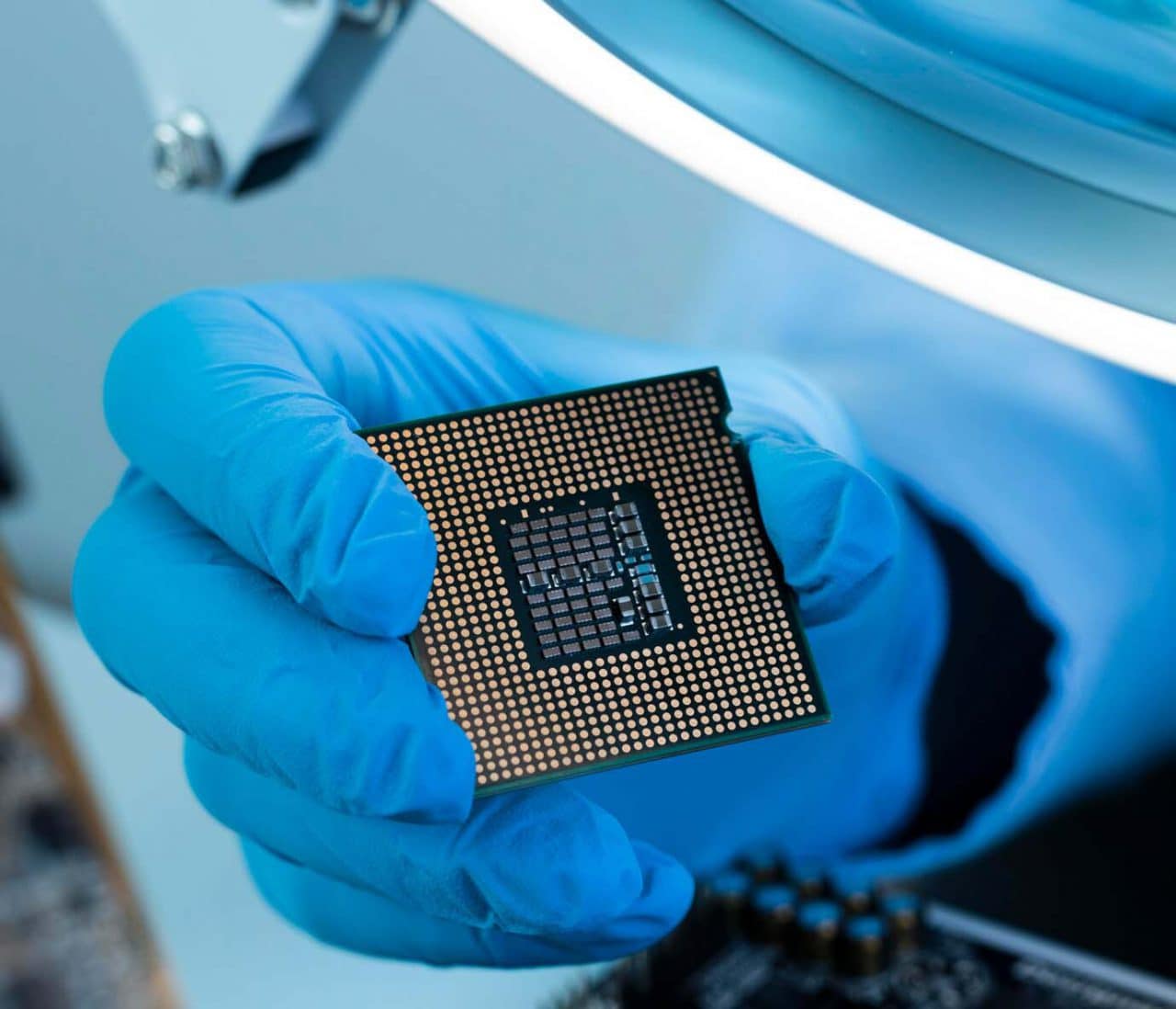
A significant part of TD Shepherd’s team has a background in the semiconductor industry, ranging from equipment and materials, fabrication, process line management to design, characterization, and test of semiconductor devices. This includes such disciplines as MEMS, (embedded) DRAM, standard cell, SRAM and I/O library design and high-speed arithmetic. Positions held by Associates cover both the technical and the marketing/sales side of the semiconductor business. Experience covers several semiconductor startups with successful exits as well as large corporates/IDMs.
TD Shepherd has extensive experience in photonics. We were part of the initial founding steps and subsequent roadmap of companies like EFFECT Photonics, a company focused on PiCs based on InP technology. We’ve advised photonics companies on manufacturing-, product- and market strategy and helped establish strategic partnerships with key players in the industry.

Neither regular semiconductors or any of its “off-shoots”, photonics or related technologies can function without the use of Electronic Design Tools (EDA). Having been part of the EDA since the early days, we understand the role it plays in the different fields and the continued innovation required to keep pace with the technologies it is serving. The continued increasing complexity, the drive for chiplets-based solutions, and the use of alternative power strategies provides enough room for startups to develop innovative solutions. Further developments on the geopolitical front create both new complexities as well as new opportunities.

The developments on the hardware level are driving continued innovation on the embedded software level. However, the developments here are much slower and mostly determined by the regular software development. Embedded software comes with very specific requirements ranging from multi-core to heterogeneous load scheduling. Startups like Vector Fabrics and Silexica were both pioneering in this field, with TD Shepherd as part of their path. Today’s innovation continues along such paths as well as developing new concepts along the AI/ML path where software is quickly becoming a distinguishing factor in the ability to demonstrate superior hardware solutions.

Like any responsible community member, TD Shepherd has evaluated its modus operandi to ensure it can make a proper contribution to becoming carbon neutral. Starting in 2022, the company has changed its travel guidelines. Priority is on trains for travel throughout Europe.
Over 2024-2026, TD Shepherd will implement a carbon compensation model to offset its travel through an appropriate compensation scheme.
TD Shepherd has and continues to contribute to the deep-tech industry through its membership of IEEE and several of its societies. We are equally pursuing the diversification of our team as a key priority. This requires a longer-term strategy focusing on growing the team in specific geographies and bringing on board new expertise.


These numbers tell our story. Uniquely for a corporate finance firm, 80% of our team have worked as engineers, so we really understand deep-tech innovation. 40% of the team have been founders of deep-tech start-ups and 30% have worked as partners or associates in a VC. This means we have a 360-degree view of business propositions and transactions, so we’re perfectly placed to support you in your next steps.
“Over 100 transactions successfully completed in the last 10 years.”
Our services will save you valuable time, effort, and expense. To streamline every transaction, we bring an established network of relevant VC, PE, and corporate partners, complemented by relationships with government bodies involved with deep-tech funding, and with independent financial and legal specialists.
“Partnering with TD Shepherd means reducing your transaction risk while accelerating the process, and an optimized outcome for all parties.”

In a nutshell: TEAM, EXPERTISE, EXPERIENCE and NETWORK. Whatever your objective, whatever your “Next Step” entails, our deep-tech expertise and network ensures a tailored approach and effective execution. Each company has its own fingerprint and, with that unique fingerprint, comes a unique strategy and execution. Not only brings our team a history of more than 100 successfully executed deep-tech projects—from M&A to fundraising to due diligence—it also brings a network across the deep-tech eco-system that is unmatched by any other corporate finance company operating in this space.
We speak your language; as a sparring partner we provide expert input and guidance on how to optimally represent the value pillars of the company, how to position it in its competitive field and how to align its roadmap with its ambition and strategy.
The TD Shepherd team will quickly understand your deep-tech proposition, help you position it clearly to attract investors, help you find the right investment partner(s), and ensure you strike the optimum deal. A partnership with TD Shepherd means you gain more time during the process to focus on your business priorities and grow your company. And as you take your next steps, our deep-tech consulting services are available to support you as your business grows.
Where we’re acting on behalf of buyers, we have the deep-tech knowledge and experience to, where and when necessary, sharpen your acquisition strategy. We are able to identify and expertly evaluate the businesses that provide the best fit for achieving your objectives while you remain at arm’s length until the best opportunity has been identified.
The TD Shepherd team will use its deep-tech experience and global contacts to find buyers with the best fit to help you achieve your goals, both at exit and post-exit. The team will work with you to position your business and to clearly communicate your value proposition. We’ll help simplify and streamline the sales process and protect your interests, giving you more time to grow your business and make it more attractive to acquirers.
An Ambition Process typically lasts weeks, preparation, execution and evaluation, specifically useful for early-stage startups and/or startups which have not yet set a clear set of goals over 3-5 years into the future.
TD Shepherd has developed a process supported by a set of tools that will help the Management Team to explore, simulate and set clear goals (the ambition) for 3-5 years out. These goals are (verifiable) realistic, supported by a set of clear KRIs and (intermediate) KPIs that help the Management Team to track the company’s performance (dashboard!) and where necessary adjust tactics and/or strategy to improve tracking and/or adjust the goals.
The Ambition Process creates a COMPASS for the Management Team to ensure directions are defined and agreed upon. Where necessary the compass can be adjusted through strategic discussion, evaluation and decision.
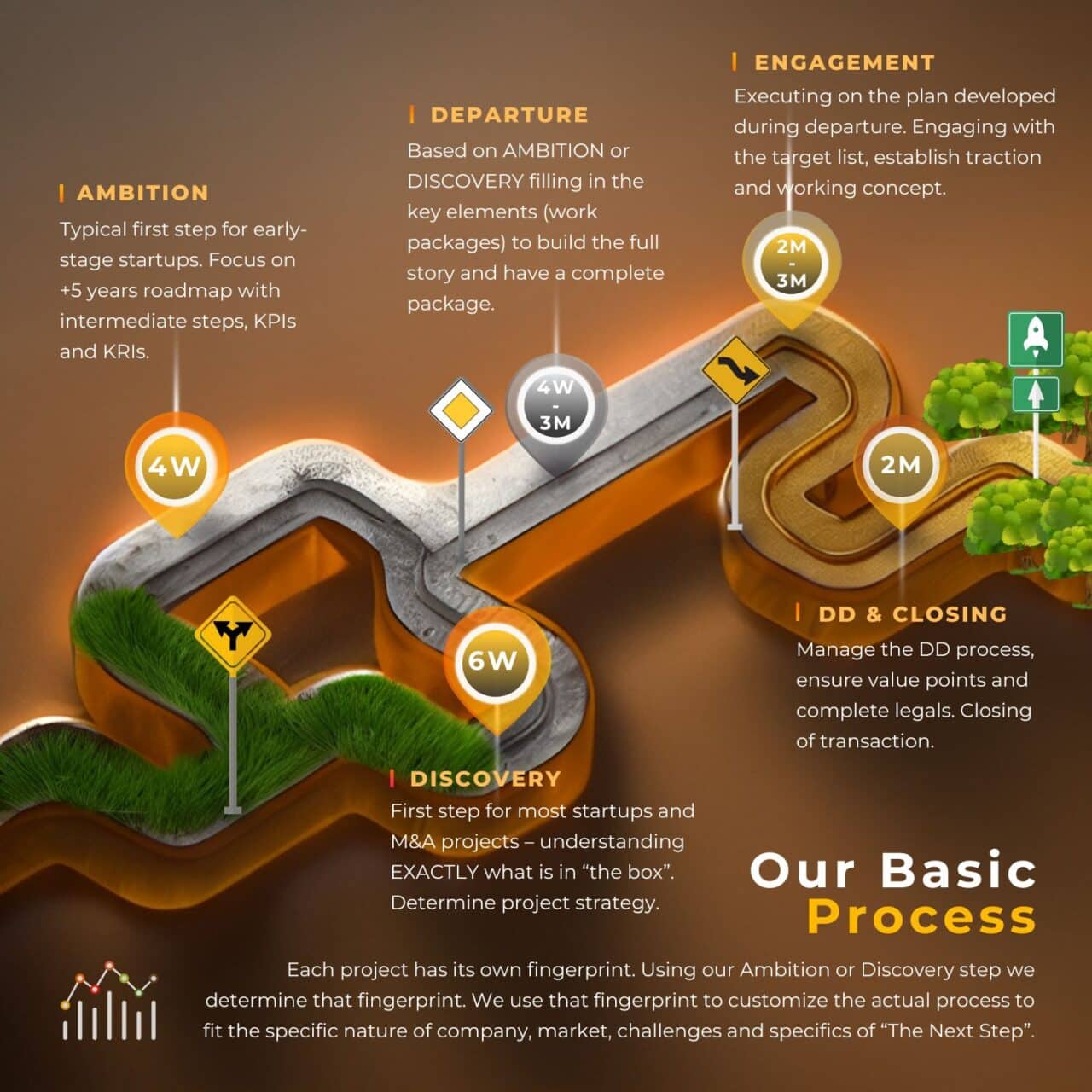
The purpose of the Discovery meeting is to determine, as accurately as possible, where the company and its management team are with respect to the clear definition and implementation of the company’s strategy, ambition, product(s), target customers, sales strategy and the financials that are the result of this. TD Shepherd takes the Management Team through a 14-step program that is customized based on the materials the Company has made available.
The first outcome of the Discovery Process is a preparedness mark that gives a generic indication as to how far the company is away from executing the Next Step.
The second outcome of the Discovery Process is the set of work packages combined with a timeline that covers what needs to be done to reach the readiness for the Next Step. The work packages and timeline are discussed and agreed on “as one team” and form the starting point for the Departure process.
The shape and form of the Departure process will vary from company to company as it is the result of the Discovery process. As no company is identical, TD Shepherd believes that the Departure process needs to be tailored to the state of the company, the needs and loading of the Management Team and the market it operates in.
Fundamentally, the execution of the Departure process, which is to complete the identified work packages, is a sliding variation between a full throttle “all hands on-board” drive to get the Company ready in the shortest possible period all the way to a monthly check, discuss-and-verify process where TD Shepherd and Management Team tick off the key tasks on a monthly basis after which a meeting takes place to review the results and discuss the next milestones and deliverables.
Depending on the nature of the “Next Step”, the Departure stage has deliverables such as investor package, 90 seconds video, acquisition memorandum, teaser and short and long list.
The focus of the Engagement process is on connecting the company with the highest ranking and best matching (corporate) venture funds. Through our network, we provide direct entry to the matching partner(s) in these (C)VCs. This achieves an expedient but also optimal closure of the funding round with a matching consortium that not only brings in the required capital but above all, a matching network that will provide a competitive edge to the Company in exploiting its market(s).
The engagement process leads towards the term sheet. Understanding the complete term sheet (“control” and “economic” aspects) in combination with the syndicate is what drives the discussion and the decision to sign a term sheet or to move on. Once the process hits the term sheet discussion, an external legal partner is brought in. Even though we fully understand the process and will continue to manage it, the legal details require a specialist. Also, as we cover the DeepTech business globally, it is imperative that each investment deal and its resulting legal documents (term sheet, Share Purchase Agreement, Shareholding Agreement, …) are judged within the local legal context.
Once a term sheet has been signed (usually under exclusivity), the process will move to the due diligence stage. As part of the Departure process, the data room has been created, vetted, and finalized. Often overlooked, a properly prepared data room is the key to smooth due diligence. This is also why we drive the data room process and ensure it is complete and up to date BEFORE the engagement process starts. From Discovery to Closing, the fundamental key is continuity: keeping the ball rolling and maintaining a positive discussion with potential investors increases the chances of success. Even though most closings, specifically early-stage closings, start with boilerplate documents, customization (and the related discussions and negotiations) is key to achieving a balanced result. This is also the reason for bringing in an external legal company to ensure proper negotiation of the detailed legal documents.
Part of what makes us such trusted advisors is our reputation for understanding the customer’s business, not just the financials. As former executives, fund managers and entrepreneurs, we bring both broad and deep experience from which we build a project team that fits the challenge. We are fortunate to have a strong team of very senior Associate Directors, who are specialists in their areas of expertise.

Starting a deep tech startup is challenging, with various hurdles to overcome. Networking is crucial for success in this space. It enables entrepreneurs to connect with like-minded individuals, investors, and potential customers.

Building a strong team for a deep tech startup involves a combination of strategic planning, effective recruitment, and creating a positive work environment.
To ensure that your startup project will grow smoothly, it is a must to attract talent and build a strong team.

Deep tech startups are at the forefront of technological advancements, creating cutting-edge solutions that shape the future. However, without effective marketing strategies, these startups may struggle to gain visibility, secure funding, and attract customers.